
This is an old revision of the document!
Photolithography
Lithography is done in one of two locations: the OSU Semi-cleanroom or CAMCOR at UO. Keep in mind the different tooling can affect the process. Further, some chemicals can negatively affect our 2D materials: WSe2 will etch in PG Remover.
To use the shared equipment in the OSU Semi-cleanrom. You can look through the big windows to see the impressive equipment. The lab is run by Chris Tasker, chris@eecs.oregonstate.edu. To use equipment in this lab you must be trained by someone in our group and then certified. Rick Presley is our main contact for certification, presley@engr.orst.edu.
The most important source of processing information is always the photoresist manufacture's data sheet see the box folder. For more technical advice you can also contact the photoresist company, MicroChem, (the company that distributes Shipley products). We have worked hard to get good/reliable recipes - some of the trials are documented.
(Moved some old_photolith_recipes)
General Photolithography Procedures
(updated 2026)
General notes:
When using a hotplate, you should not assume it is hot enough just because the indicator says it is. See below:
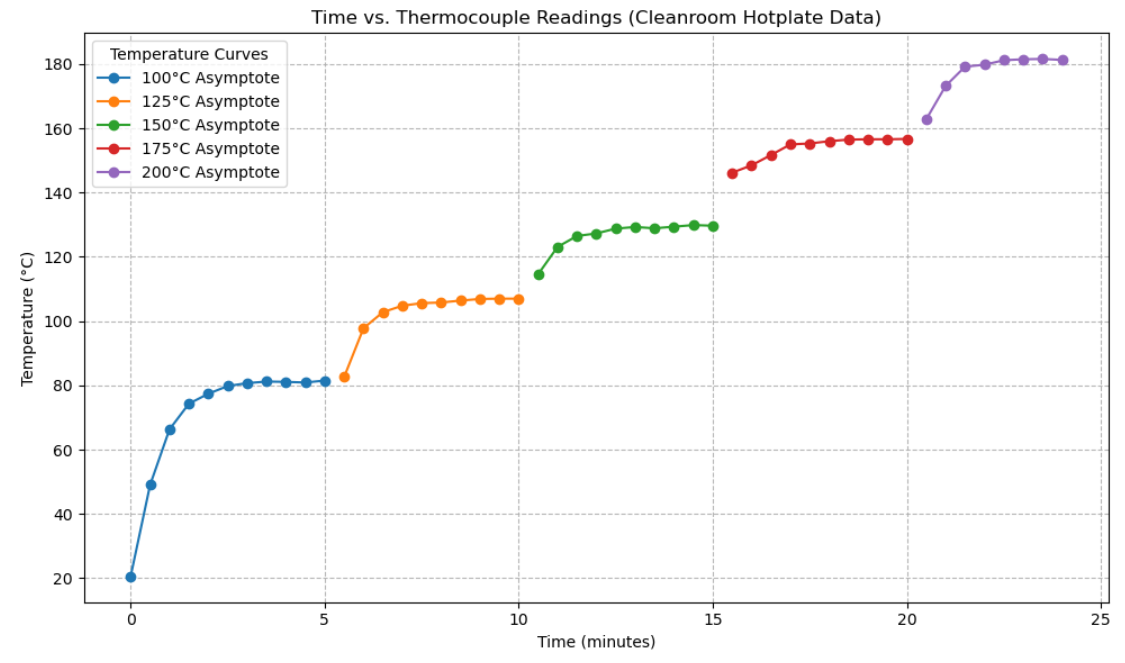
When referring to temperatures, we will refer to the displayed temperature, but notice that these are not the same as the actual surface temperature. We have thermocouples which allow us to check the surface temperature in our lab and in the cleanroom drawer. Gus also keeps one at UO for spinning resist at CAMCOR.
(I) Preparing your substrate
We typically prebake our substrates to remove water from the surface before spinning them with resist. We have two temperatures that we use for this:
- 180 C: bake for 2 minutes
- 115 C: bake for 3 minutes
Pick whichever matches the next temperature you need for your resist soft bake to avoid having to wait for the hotplate to heat/cool.
(II) Spin-coating
Members of the lab have enjoyed using the Laurell spin coater. It is also very common across other labs. Request this spinner specifically when training with Rick.
We typically will use single or bilayer resist stacks. If you are working with bilayer resist, you will repeat this section for each photoresist applied and use the relevant parameters for each (see below)
- Set you spin parameters in the spinner.
- Blow off your substrates (do this for every layer if you don't have 2D materials on the substrate -Gus)
- Load your substrate onto the vacuum chuck. Use the largest chuck which does not cover more than ~80% of the bottom of the sample. This helps prevent vacuum leaks or resist being pulled into the vacuum.
- Cleanly pipette resist onto center of chip. Immediately spin for 45 s.
- Place chip on the center of preheated hotplate for requisite time.
Processing Parameters:
LOR3A:
- Spin speed: 4000 RPM, 1000 rpm/s ramp rate
- Spin time: 45 s
- Bake temperature: 180 C
- Bake time: 4 minutes
The etch rate of the LOR is highly temperature dependent. See the data sheet for details.
S1818/S1813:
- Spin speed: 4000 RPM
- Spin time: 20 s
- Bake temperature: 115 C
- Bake time: 2 minutes
S18XX is a product line where the last two digits represent the nominal thickness of the resist (it still depends on spin parameters, see datasheet) S1818 is expected to be 1.8 μm for example.
Edge bead removal for the mask aligner:
The edges of the chip will have built-up photoresist that is many times thicker than the rest of the chip. Edge bead removal is particularly important for fine features on small substrates, as edge beads prevent the chip from fully contacting the mask.
Try putting a tiny amount of Remover PG on the tip of a swab and wiping it on an alphawipe, then swab your edges at a 45 deg. angle to remove edge beads.
(II) Exposure
Depending on the tool you use, the process and logistics will be different. We currently lack good documentation for:
- The mask aligner in MASC
- The direct write tools in CAMCOR
Cross contamination
- Be extremely careful when using CD-26 & MF-351 in the same lab. One drop of MF-351 in a gallon of CD-26 ruins the whole gallon! This problem was so bad that Shipley built a separate facility just to keep these away from each other.
Photoresist removal
Matt has documented that hot PG remover leaves less PR residue than any other method we have tried.
We are also currently working on developing a good process for cleaning up chips after lithography using AFM cleaning or O2 inductive plasma (barrel ash).