Table of Contents
Outreach
Internet resources
- Index of university-level lecture demonstrations from University of Maryland.
- Index of hands-on science activities from the Exploratorium
- Popular demos commercially available from Steve Spangler Science
Some other fun videos:
- The chain fountain explanation. Inspired by Mould's video that was posted in 2013. Theory paper published soon after. Picked up by NY Times in 2014.
Workshops
- Peak Adventure Club - The Physics of Air (1/11/2015)
- 2012 SMILE workshop Nanoscience activities for the High School Classroom (8/8/2012)
- Saturday Academy (7/20/2011), http://photobucket.com/MinotOutreach7-20-2011
SESEY
Summer Experience in Science and Engineering for Youth SESEY.
Ideas for 2018: Photolithography mask design. Transparent electronics on glass slides using graphene. Prove conductance. Measure transparency. A Day Made of Glass
| Project Year | Project Title | Participants | Summary |
|---|---|---|---|
| 2019 | Build a microscopic oxygen sensor for nanotech research | Quinn and Kiara | You'll get hands-on experience building microscopic structures, and using measurement tools for the microscopic world (scanning electron microscopy and atomic force microscopy). You'll calibrate the sensor to monitor encapsulated bacteria that have been engineered to clean up ground water. |
| 2018 | Build a nanoelectronic device | Shelby and Kevin | You will build a nanoelectronic device out of a single sheet of graphene. You'll get hands-on experience building microscopic structures, and using powerful measurement tools like scanning electron microscopy and atomic force microscopy. |
| 2017 | Graphene nanotechnology | Chris and Ian | You will build a nanoelectronic device out of a single sheet of graphene. You'll get hands-on experience building microscopic structures, and using powerful measurement tools like an atomic force microscope. |
| 2016 | Nanotechnology: Carbon-based electronics | Ryan and Deven | You will build a transistor out of a single carbon nanotube. First we'll build an accurate scale model of the transistor, then we'll make the real thing. You'll get hands-on experience with the same processes that are used to make computer chips, and with microscopes that are powerful enough to see carbon nanotubes. |
| 2015 | Nanotechnology: Carbon-based electronics | Evelyn and Polina | You will build a transistor out of a single carbon nanotube. First we'll build an accurate scale model of the transistor, then we'll make the real thing. You'll get hands-on experience with the same processes that are used to make computer chips, and with microscopes that are powerful enough to see carbon nanotubes. |
| 2014 | Nanotechnology: Carbon-based electronics | Trey and Malerie | You will build a transistor out of a single carbon nanotube. We'll start by making an accurate scale model the transistor and then make the real thing. You will be guided through the same high-tech processes that are used to make computer chips. Once completed, you'll get hands-on experience with microscopes that are powerful enough to see carbon nanotubes. |
| 2013 | Nanotechnology: Carbon-based electronics | Stephanie and Yan | You will build an electrical circuit out of a carbon nanotube. We'll start with a hands on model of the circuit making process to show you some of the science behind nanoscale electronics. The next step is making the real thing. With the mentor's help you will go through the fabrication process which includes 1) Carbon Nanotube Growth, 2) Circuit patterning, 3) Depositing Metal Electrodes - these fabrication steps are also used by companies like Intel to make computer processors. Once completed, you'll get hands on experience with several special types of microscopes that allow you to “see” the carbon nanotubes which are so small that they are invisible to standard optical microscopes. |
| 2012 | Nanotechnology: Carbon-based electronics | Megan and Arek | You will build an electrical circuit out of a carbon nanotube. We'll start with a scale model of the process which you can build on your own, then move onto the real thing (chemical vapor deposition, photolithography, metal evaporation). Once you've made a circuit, you will get hands-on experience with several microscopes that allow you to see the carbon nanotubes (carbon nanotubes are so small that they are invisible to standard optical microscopes). |
| 2011 | Nanotechnology: Carbon-based electronics | Madeline and Elizabeth | You will build an electrical circuit out of a carbon nanotube. We'll start with a scale model of the process which you can build on your own, then move onto the real thing (chemical vapor deposition, photolithography, metal evaporation). Once you've made a circuit, you will get hands-on experience with several microscopes that allow you to see the carbon nanotubes (carbon nanotubes are so small that they are invisible to standard optical microscopes). |
| 2010 | Atomic force microscopy of carbon nanotubes | Claire and Ryan | The atomic force microscope (AFM) has revolutionized science by allowing researchers to “see at the nanoscale”. In this project you will learn the principles of AFM imaging by using a working model of an AFM. This model AFM has been built so that all the parts are big enough to see in action. Once you understand the principles of AFM imaging, your mentor will help you use a real AFM to see carbon nanotubes. |
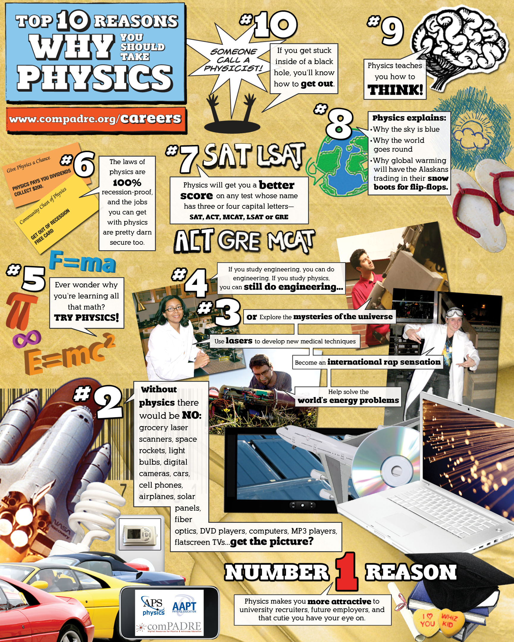
Careers in Physics
 | Poster from the AAPT website |
Find out the career statistics of recent physics graduates, see the reports from the American Institute of Physics
Physics demo shows
Air
- Hovercraft (leaf blower)
- Floating beach ball (similarity with laser trap)
- Fill bag with one breath (entrainment)
- Drop paper cones experiment
- Vacuum bell jar (marshmallows, balloons)
- Air cannon
- Crushing soda cans
Optics
- Gas discharge lamps with Ne, He etc., viewed with diffraction glasses
- Michelson Interferometer (relate to gravity waves)
Particle physics
- Cloud chamber
Materials physics
- Floating superconductor (needs liquid nitrogen)
Central forces
- Swinging a pale of water
- Rotating chair
Density/buoyancy
- Fish tank of water, Coke can sinks, Diet Coke floats, prediction for grapes?
Oscillation and waves
- Range of human hearing (sound waves)
- Wave machine
- Standing waves on a rope
Thermal
- Sterling engine
Electromagnetism
- Van der Graf generator
- Jacobs ladder (connect to lighting, connect to speed of sound and measuring distance)
Movies:
- Tacoma Narrows bridge collapse
- Myth busters car crashes
- High frame rate slow motion videos
Outreach resources
- Nanoscale Informal Science Education (NISE) Network - Includes a collection of hands-on nanoscience activities.
- Video of the FIB lift out technique for preparing TEM samples.
AFM kits
Bring along:
- laptop
- CNT model
- Scissors
Teaching resources
- Best practices for using clickers in the classroom: collection of videos
- Best practices for creating a social/functional research group: APS report
 | Graphene lattice ready to be printed on transparencies and cut into smaller pieces so that participants can roll carbon nanotubes of various chiralities. |
 | High resolution image of a graphene lattice |
Gold Wire Experiment
This activity uses two gold wires to demonstrate quantum effects in electron transport. When the wires are in contact with each other and a voltage source a current will flow through the completed circuit. But as the wires separate from one another, a small junction of gold atoms forms keeping the wires electrically connected for a brief time. This junction pulls apart similar to silly puddy where the material thins down until it breaks. When the gold junction thins down less atoms are contributing to carrying a current. This leads to discrete drops in the measured circuit current that correspond to single or small groups of gold atoms breaking off to one side of the stretched out junction. A power point explanation of the experiment can be found here.
 | Photo of Setup. |
 | Measured current steps during break process. |
 | Metal Cover helps shield outside sources of electrical noise. |
 | The gold wires are mounted in place. One of the wires is attached to a micromanipulator to help position the wires. |
 | A homemade current preamplifier turns the circuit current into a scaled voltage that is measured with an oscilloscope. |
 | Front of electronics box with power switch and bnc outputs. |