start
Welcome
Welcome to the wiki for the Minot Research Group in the Department of Physics at Oregon State University. Group members contribute and maintain up-to-date manuals, recipes and information on many common lab questions. (Setting up a wiki like this one is relatively easy.)
Image Gallery
You are welcome to use our images for a class or presentation, please reference “Minot Group, Oregon State University”.
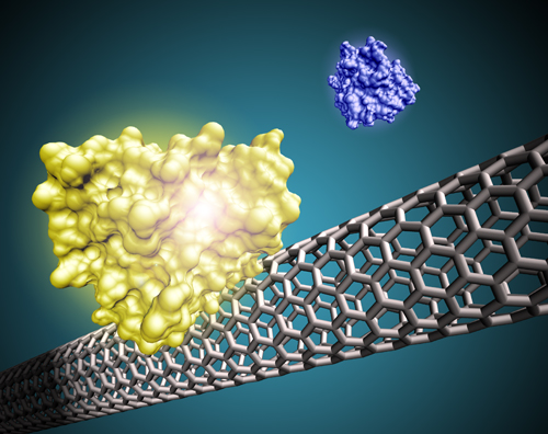 | Proteins tumbling in solution and binding to a nanotube. Binding events like these can modify the nanotube's resistance, allowing the device to be used as an electronic biosensor. We study the way these sensors operate and what they can accomplish. Hopefully, in the future, inexpensive biosensors devices will be available to rapidly/accurately analyze blood samples. Image by Landon Prisbrey. |
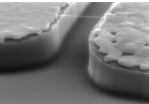 | A suspended carbon nanotube bridging the gap between a pair of electrodes. The CNT diameter is about 2 nm, it is hanging about 1 micron above the oxide surface. We submerge these devices in liquid environments and introduce biological molecules such as single-stranded dna. Our experiments test the physical mechanisms involved in electronic biosensing, and push the limits of detection speed and sensitivity. Image by Tal Sharf. Fabrication by Tal Sharf and Josh Kevek. |
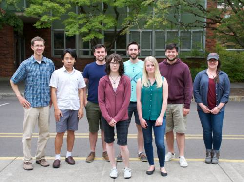 | Research group in Summer 2019. From left to right: Ethan Minot, Duy Nguyen, Daniel McCulley, Carly Fengel, Dublin Nichols, Hanna Hansen, Mitchell Senger, and Olivia Clark. Group photos from previous years. |
 | Using spectrally-resolved photoconductivity it is possible to identify the chiral index of individual semiconducting CNTs. Image by Tristan DeBorde. See our 2014 paper in JPCC. |
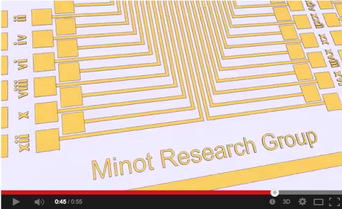 | Fly-by tour of a carbon nanotube field-effect transistor chip by Tristan DeBorde |
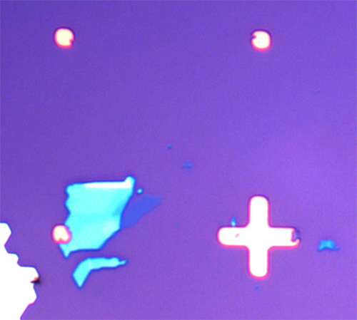 | Optical microscope image of exfoliated molybdenum disulfide (MoS2) on an SiO2/Si wafer. A grid of gold alignment markers frame the image. There is a 2 x 5 micron flake of single layer MoS2 near the bottom left alignment marker. Image and sample fabrication by Lee Aspitarte. |
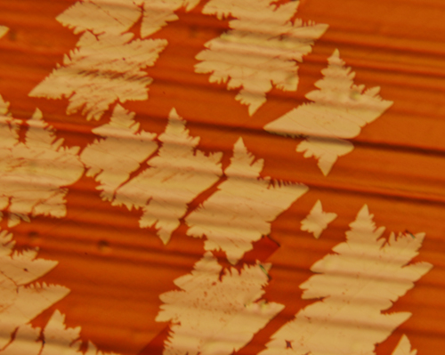 | Optical microscope image of graphene grown on copper foil. The pieces of graphene (about 100 micron in size) have flower-like geometries. The graphene film is one atom thick, but is still able to prevent oxidization of the underlying copper. Red areas are oxidized copper, yellow areas are not oxidized. |
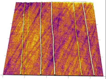 | Atomic force microscope image (2 micron scan size) of single walled carbon nanotubes (~ 1 nm tall) grown on a quartz substrate. Van der Waals interactions between the nanotube and the crystalline substrate determine the preferred growth direction. Image by Josh Kevek. |
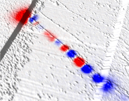 | Photocurrent response from a CNT. The figure shows the surface of a CNT device (as measured by AFM). The surface has been colored to indicate the photocurrent response of the circuit. The steps in surface height correspond to the metal electrodes that contact the CNT. The gap between the electrodes is 10 μm. The blue dots are regions where negative photocurrent was induced by the scanning laser (2 mW, 632 nm). The red dots are regions where positive photocurrent was induced by the scanning laser. Image by Tristan DeBorde |
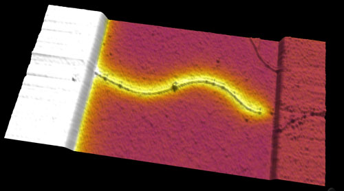 | Carbon nanotube connected to a metal electrode at V = -3V. Color contrast is a map of the electrostatic forces between the sample and the grounded AFM tip. The gap between the electrodes is 3 μm |
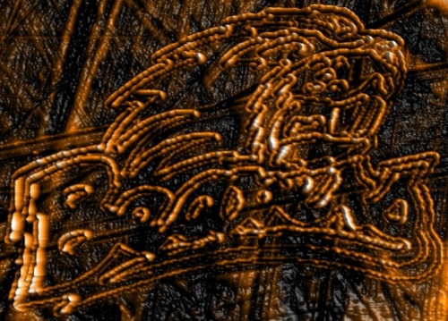 | Oregon State Beavers' logo scratched on a plastic layer, 7 x 10 μm atomic force microscope image. This is the smallest beaver ever made at OSU, but not the smallest Beaver logo ever made. Dr. Keizler's group in Chemistry holds the “smallest ever” award. They used the ebeam facility in Eugene. |
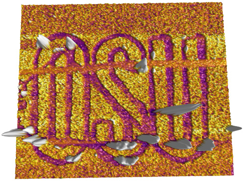 | 3 micron scan of proteins coating a silicon oxide substrate. The proteins have been pushed around by the AFM tip to form the OSU logo. The proteins pile up during the writing process, like snow on the side of a ploughed road. The surface roughness corresponds to individual proteins, the individual protein molecules are 4 nanometers tall |
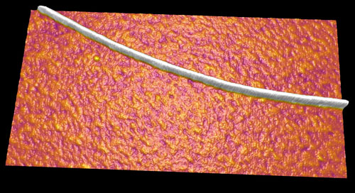 | Carbon nanotube grown on silicon oxide, 400 x 800 nm AFM scan |
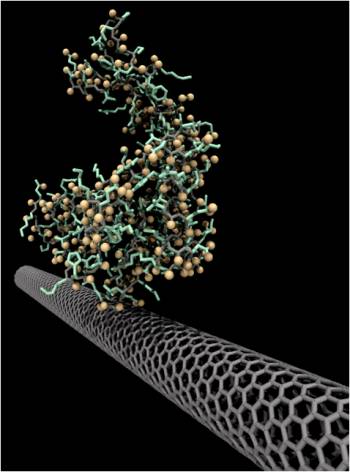 | Adenylate Kinase attached to a nanotube. We are working on ways to realize this geometry in real life. We hope to 'listen' to the enzyme move in real time by monitoring the nanotube's resistance. Are protein conformational changes big enough for us to detect? We are answering this question by modeling the protein and electrolyte & then numerically solving the Poisson-Boltzmann equation. Image by Landon Prisbrey. |
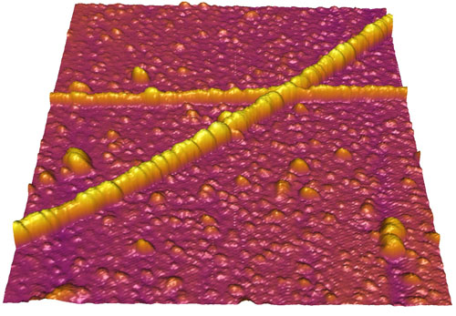 | 1 micron scan of IgG proteins on top of nanotubes. We are currently investigating how protein binding effects the conductance of nanotubes. This biosensor technology is a promising route to improving medical diagnostics. |
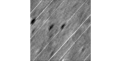 | 2 micron scan of aligned SWNTs growing across the surface of ST-cut quartz. The nanotube growth direction is controlled by atomic steps (not visible) in the quartz substrate. This growth technique was introduced in 2007 and solves many issues that were limiting high-yeild manufacturing of nanotube devices. |
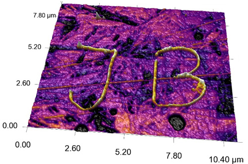 | Write you initial where nobody can see! The substrate is a CD. The plastic coating is perfect for doodling with an AFM tip. |
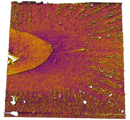 | 5 micron scan showing a flake of single layer graphene (0.5 nm tall). Graphene is a sheet of covalently bonded carbon atoms which is one atom thick. Graphene has unique electrical properties such as zero effective electron mass. Sample courtesy of Lan Liu, TU Delft. |
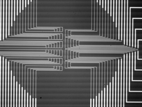 | Optical microscope (~ 2 mm field of view) showing the electrodes for 50 different nanotube devices. The layout is designed to fit a 1 mm o-ring around all active transistors. |
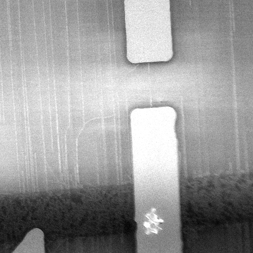 | SEM image of an aligned nanotube bridging the gap between a pair of electrodes. Electrode width and transistor channel length are 10 microns. Thanks to Kurt Landworthy at CAMCOR for assistance with imaging. |
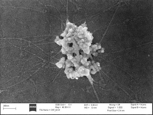 | SEM image of an alumina nanoparticle which is used to support CNT catalyst. A large number of CNTs are seen growing from the catalyst particle. Thanks to Kurt Landworthy at CAMCOR for assistance with imaging. |
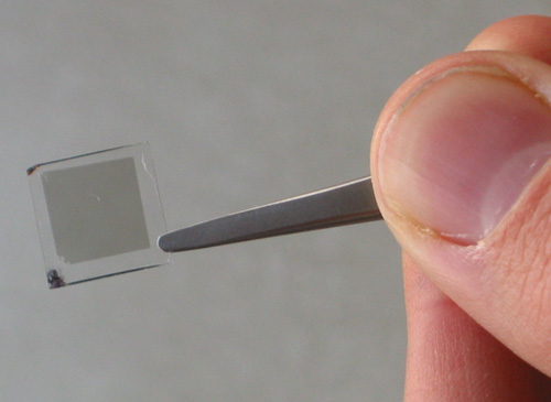 | Sample courtesy of Leo Fifield, Pacific Northwest National Labs. Nanotubes were first dissolved in solvent, then caught in a filter and then pressed on this glass substrate. In the grey square the nanotubes form a mat many tubes deep. We collaborate with Dr. Yun-Shik Lee (OSU Physics) to study the optical and THz properties such samples. |
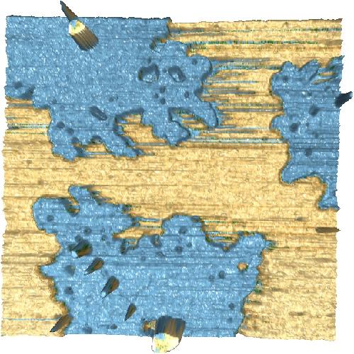 | 4.5 micron AFM image of mycobacterial membranes taken in liquid. The membrane has separated into two phases, the step height between the two phases is approximately 1 nanometer. The image has been colored using the relative energy dissipation of the AFM tip tapping on the softer phase vs. the firmer phase. The sample was prepared by Raghu Parthasarathy's group (Department of Phyiscs, University of Oregon) who study the dehydration resistance of these membranes (2008 article in Biophysical Journal.) |
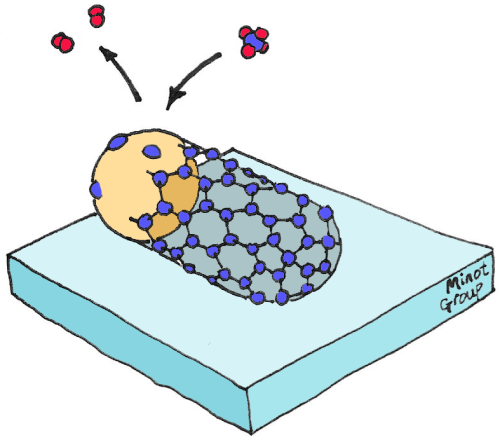 | Cartoon of the chemical vapor deposition (CVD) growth process for carbon nanotubes. The orange sphere is an iron nanoparticle, the substrate is quartz. The growth is carried out at 900 degrees Celsius in the presence of methane and hydrogen gas. |
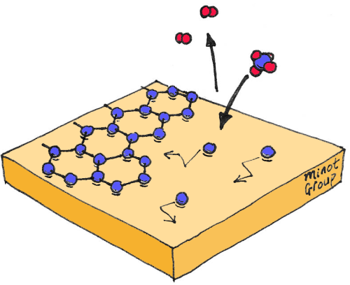 | Cartoon of the growth process for CVD graphene. The orange substrate is copper foil. The growth is carried out at 1000 degrees Celsius in the presence of methane and hydrogen gas. |
start.txt · Last modified: 2019/10/19 11:18 by ethanminot
