Table of Contents
Probe Station
LabVIEW
We use labview programs to control voltage sources and acquire data. For documentation on the MeaSureit program see Vera's program development site. It is straightforward to use programs that are already written. If you need to write your own labview program, it will take some time investment to learn this graphical programming language. The time is well spent because labview the industry standard for software control of processes. There are tutorials, videos and exercises on the labview website and further material at labview for students section. On the T: drive there is a folder Manuals/Labview where we keep some example programs.
More information:
Avoiding damage
Nanotubes burn up like a fuse if currents get too high (above 10 microAmps in a single tube starts to be dangerous). If the gate oxide is stressed, it can also be irreversibly damaged. This can happen several ways.
- Electrostatic discharge (especially dangerous with quartz substrates). To avoid this, always ground yourself with a grounding strap when working in the probe station.Your body is like a van der Graph generator when insulting shoes walk across an insulating floor. Quartz substrates are also insulting, so the circuit on top of quartz can build up significant charge while it sits in the box - I don't know how (cosmic ray ionization?), it just does.
- Sudden large jumps in the source/drain or gate voltages stress the gate oxide and lead dc currents and/or capacitive currents through CNTs. Voltage jumps could happen by (i) having intermittent contact between a probe needle and the backgate, (ii) Landing a source/drain probe needle on a floating contact pad without first zeroing the gate voltage, (iii) accidentally telling the computer to jump the gate voltage.
- Electromagnetic pulses from high power electronics (e.g. a CRT tv screen being turned on).
- The resilience of the SiO2 layer is better if it has never undergone high temperature processing (like CVD growth or anneals). Other labs (Ji-Yong Park, Brian Leroy, etc.) minimize the amount of high temperature processing to avoid damage to the oxide.
- The SiO2 layer is also compromised by exposure to salty water because the ions penetrate the oxide and make the oxide conductive.
- If there are mechanical switches in the CNT circuit, it is best to use a "make and break" switch system.
Sampling
To collect quality data at fast sampling rates there are many points to consider
- Frequencies up to the Nyquist frequency are 'high quality' and contain useful information. The Nyquist frequency is half the sampling rate. This means that if you want to measure a 20 kHz periodic signal then you need to at least need to sample at 40 kHz in order to resolve it. Sampling even faster than 40 kHz would make the data at 20 kHz more reliable. This is an example of oversampling and is good practice to avoid artifacts.
- Some equipment will have a bandwidth limit (essentially a built in low pass filter). The bandwidth of the Stanford current amplifiers in the lab are a function of the gain mode you use:
- Sensitivity ⇒ Bandwidth (3 dB) (in High BW mode)
- 1 mA/V ⇒ 1 MHz
- 100 μA/V ⇒ 1 MHz
- 10 μA/V ⇒ 800 kHz
- 1 μA/V ⇒ 200 kHz
- 100 nA/V ⇒ 20 kHz
- 10 nA/V ⇒ 2 kHz
- 1 nA/V ⇒ 200 Hz
- 100 pA/V ⇒ 100 Hz
- 10 pA/V ⇒ 20 Hz
- 1 pA/V ⇒ 10 Hz
Standard operating procedure
Silicon substrates
- Ground yourself with a wrist strap then take the chip out of the box.
- Start up meSurit and set the source drain voltage to 10 mV (remember there may be a voltage divider in the circuit).
- Cross the source and drain needles like swords and check that current overloads.
- Touch the two needles to the same pad on a chip and check that current overloads. If it does not, clean the probe needle tips.
Quartz substrates
- Ground yourself with a wrist strap then take the chip out of the box.
- Attach a probe needle to ground via a 10 MOhm resistor.
- Touch the probe needle to every pad that you plan to use. Built up charge will slowly discharge (I guess the time constant of the RC circuit is < 1 second, but someone should calculate).
Applying a Gate Voltage
Three ways to apply a gate voltage to a silicon/silicon oxide chip:
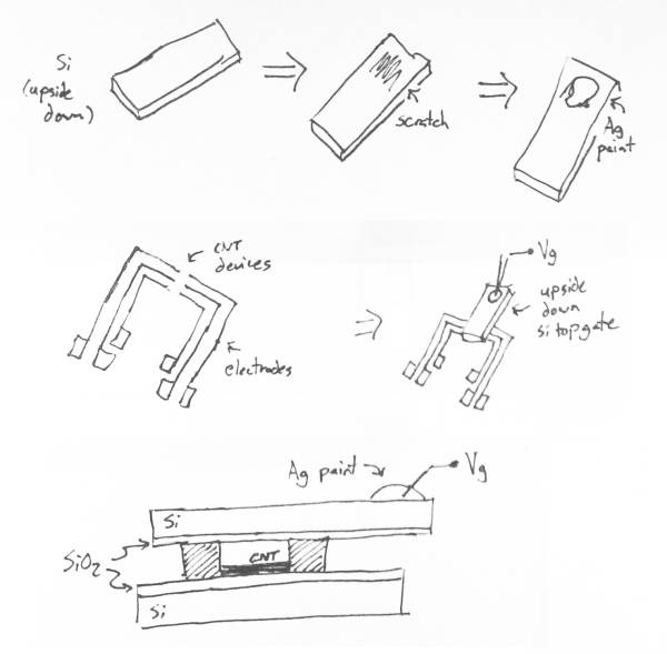
- Place the chip on a conducting surface (a piece of copper on top of a piece of glass, a glass slide painted on one side with conductive paint, a covered in a thin film of evaporated metal). The conducting surface must be isolated from all other conductors. The surface will contact the silicon underside of the chip and apply a gate voltage to the entire chip.
- Scratch a hole in the oxide layer of the silicon and place the probe on the scratch. In this method you also need to place the chip on a glass slide to avoid grounding the chip.
- Water gating: see Using the fluid cell below.
It is important to sweep the gate voltage in a continuous fashion, rather than instantaneous jumps. Fast switching puts stress on the insulating dielectric (the silicon oxide). If the insulating dielectric breaks down, large currents will start leaking between the gate and the top electrodes.
Gate Leakage
If you put a positive bias on the nanotube, the current throught the tube should always be positive. If you see negative currents as you sweep the gate voltages, something is suspicious. Three possibilities
- Charge is leaking from the gate into the metal electrodes. Check this by lifting the lifting the micromanipulator that applies the source voltage to the nanotube, and see if current changes as a function of gate voltage. These leakage currents will increase with gate voltage.
- A small capacitive current (~ 1 nA) is seen because you are sweeping the gate very quickly (~ 1 V/s). Capacitive currents are still present when you lift the micromanipulator that applies the source voltage to the nanotube. This current is proportional to dVg/dt and does not change with Vg.
- If the chip is underwater and you are doing watergating (see below), you might be observing electrochemical reactions occuring at the water-electrode interface. Note that the electrode surface area is much larger than the nanotube surface area. Therefore, elecrochemical currents picked up by the electrodes are typically much larger than electrochemical currents picked up by the nanotube.
Using a Top Gate
Using a top gate is a convenient way to obtain an I(Vg) measurement from a device with (1) no 'back gate' (such as quartz) or (2) with damaged gate oxides. Over time, leakage through the gate oxide will become significant. A common cause of this is when metal nanotube catalyst 'diffuses' into the oxide layer (timescales ~ weeks/months), forming conductive 'filaments' through the oxide. In this case, I(Vg) curves can still be obtained by using a top gate. The top gate has a lower capacitive coupling to the devices compared to a built-in back gate. The rule of thumb is ±10 V on the back gate corresponds to about ±30 V on the top gate (empirical estimate using 300 nm oxide) .
Important: Be sure that the silver paint area does not overlap any electrodes underneath. Ions in the paint will diffuse through the top gate chip over time, forming conductive 'filaments' that lead to top gate leakage. If you are sure to follow this step, top gate ranges ±100 V should be easily achievable.
Noise
The current through a CNT or graphene device will always fluctuate due to 1/f noise. This noise is intrinsic to any electrical measurement we perform. However, other types of noise which are unrelated to the device need to be minimized. External noise sources typically show up as spikes in the power spectral density of current fluctuations. In the most extreme cases, you can actually see sinusoidal oscillations in your current measurement.
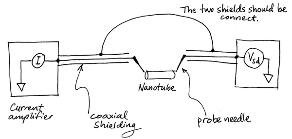
The most common reason for unusually high noise can be fixed by connecting the shield on the BNC wires which carry source, drain and gate signals (see Figure below).
Rules of Thumb
- Work in an area completely surrounded by grounded metal (like a Faraday cage)
- Be sure to use a DC light source inside the box (such as LED lighting). Also, be sure that the AC to DC conversion for the lighting happens outside the box.
- As a rule, keep AC voltages out of the Faraday cage unless they are required for the measurement.
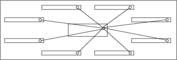
- Ensure you don't have any 'ground loops'. Faraday's law of induction, tells us that closed loops of metal will 'catch' stray EM waves and give you pesky EMF currents (noise). For this reason, it is better to use a 'star ground' system, rather than a 'daisy chain'.
- More details: Grounding the chassis of all electrical components in a star configuration is a common technique for eliminating ground loops and therefore minimizing pick-up of EM radiation. There is one central ground, with a wire radiating out to each piece of equipment. In its simplest form, star grounding means that you plug all measurement equipment into the same powerstrip on the wall. It is important to keep the ground on this power strip as quiet as possible. For example, the computer monitor should be plugged into a different power strip (different circuit).
Using the fluid cell
Tips
- Liquid gate electrodes may be fabricated directly on the microchip. Some of our fluid cell designs incorporate a hole to insert a liquid gate electrode which is independent of the chip (called a reference electrode). The reference electrode we use is RE-6 from Bioanalytical systems. A manual is available. It is critical that the electrode is always wet, and always stored in 3M NaCl solution.
- Liquid gating is more effective than back gating because electrolyte surrounds the nanotube. Smaller gate voltages are required. In general use a factor of 10 less (+/-500 mV is safe).
- Before using a syringe flick the top like a nurse to get rid of any bubbles
- Before loading a syringe pump some liquid into the hole first. When pushing the syringe in place some liquid should leak out the sides. This prevents bubbles from getting into the system.
- Use clean room towels to dry the fluid cell
Walkthrough
This walkthrough describes how to set up a fluid cell for use with a PDMS stamp and and on-chip liquid gate electrode.
- Ensure that fluid carrying components are clean
- Sonicate fluid cell and tubing in ethanol for 20 min
- PDMS stamp cleaning procedure
- 20 min bath in hexanes (PDMS will swell to 2x their normal size)
- 20 min bath in IPA
- 5 min sonication in ethanol(?)
- Spray rinse DI water
- Nitrogen blow dry
- Get out the plastic fluid chuck plate (with the micromanipulator attached) and it's box with attachments and accessories
- Affix the microchip slide attachment to the micromanipulator on the fluid chuck plate
- Clean the microchip slide with ethanol on a beta wipe
- Adjust the micromanipulator's z screw until the microchip is fully raised
- Stick the PDMS stamp to the underside of the microchip slide (with the channels facing down), and place your microchip beneath on the chuck plate.
- Put the whole assembly in the probe station
- Use the probe station's microscope and the micromanipulator's x, y, and z adjustments to precisely place the PDMS stamp onto the microchip to ensure that the microfluidic channel will guide liquid over your sensors.
- When the PDMS stamp is placed, gently push down on the stamp with tweezers to ensure a good seal with the chip
- Raise the micromanipulator's z adjustment to maximum height and remove the PDMS stamp from the microchip slide
- Remove the fluid chuck plate from the probe station
- Replace the microchip slide attachment with the fluid cell
- Place the microchip+PDMS stamp underneath the fluid cell
- Use the micromanipulator's x, y, and z adjustments to precisely place the fluid cell onto the PDMS stamp. Be careful to ensure that the fluid cell's channels align with the wells in the PDMS stamp.
- Move the fluid chuck plate to the probe station
- Attach the fluid cell's input fluid line to the output from the fluid channel selection switch (near the back of the probe station)
- Tape the fluid cell's waste line above a waste container
- Do not dip the waste line into the waste fluid. Potential variations in the waste fluid can be communicated upstream to your device and potentially dope your FET.
- Connect a syringe to a fluid channel, and ensure that the fluid selection switch inside the probe station is set to the correct fluid channel
- Place the syringe in the fluid pump, and begin pumping
- Watch the fluid cell channels and waste line for evidence of fluid moving through the system. If no fluid moves, or if liquid begins to pool around the microchip, then the line must be plugged somewhere. Often this happens when the fluid cell channels were not properly aligned with the PDMS stamp wells.
- Connect the drain and liquid gate electrodes
- Sweep the liquid gate electrode over about ±500 mV. Watch for parasitic Faradaic currents which imply electrochemistry is taking place (don't let the currents exceed 1 nA).
- Identify your liquid gate 'working region'. This is the V_lg region where parasitic currents are <1nA. In this region capacitive currents dominate. Your IV curve should be nearly flat, and the current value depends on the direction and speed of the gate voltage sweep.
- Connect the source electrode and perform your experiment
- When finished, store PDMS stamps between two microchip coverslips. They may be re-used following the cleaning procedure listed above. New PDMS stamps are fairly easy to make, so don't feel afraid to throw them away if in doubt about their integrity.
Local liquid gate techniques
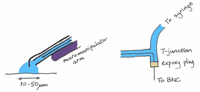
Jaan Mannik developed the following local liquid gate technique:
Tubing is secured to the arm of a micromanipulator. A thin Pt wire is inserted into the tubing. The wire comes out of the tube after passing through a T-junction. The wire inside the tubing is called the working electrode. A voltage is applied to the working electrode using the DAQ.
A second Pt wire is on the outside of the tubing. This is called the reference electrode. This outer Pt wire can be used to record the actual potential of the liquid (sometimes it is different than the voltage applied to the working electrode). The voltage signal can be sent straight to the DAQ.
Megasweeps
A 'megasweep' is when you scan the source-drain voltage (Vsd) and gate voltage (Vg) while recording current (I) through the device. This allows you to make a three dimensional plot, usually with Vsd on the y-axis, Vg on the x-axis, & conductance or the differential conductance (dI/dVsd) on the z-axis.
- Green Box
- In meaSurit sweep Vsd & Vg to their starting values
- Click on the 'Multi Scan' tab
- From the 'Scan channel' dropdown menu choose 'Vsd'
- Vsd will now be scanned 'fast'
- Verify that 'Vg' is selected in the 'Scan Channel 2' dropdown menu
- Vg will now be scanned 'slow'
- Set 'delay 2' to 0.5.
- This will add a 0.5 second buffer in between Vsd scans. Without a time buffer you can 'see' the device adjusting to the big Vsd change at the beginning of each line (which is not good).
- Purple Box - Setting the scan parameters
- Set the max and min values for Vsd and Vg
- Set the step sizes ΔVsd and ΔVg
- These must obey a couple of rules of thumb. First, remember the nanotube will feel the full force of Vsd, but the effect of Vg will be screened by about 100x before reaching the nanotube. So make 1 pixel in the Vsd direction approximately the same effect as 1 pixel in Vg by using ΔVsd = ΔVg/100.
- Another rule is that meaSurit can only record about a 39,000 pixels^2 image before it crashes. For this reason we'll make a second rule: (Vg range/ΔVg)* (Vsd range/ΔVsd) = 39,000
- Now we have two equations and two unknowns so we can solve to find the appropriate step size for our image: ΔVsd = 5.06E-4 * sqrt(Vg range * Vsd range)
- Set the steps per second for the fast (Vsd) scan
- Make sure the setting used here makes sense with the current amplifier settings you use
- Pink Box
- Set the 'path' for the saved megasweep data
- Set the filename
- Click the 'autosave' checkbox
- Green Box
- Click 'start'
- The time it takes to complete the megasweep is given by: time = [Vsd range/(ΔVsd*scan rate) + delay time] * (Vg range*100/ΔVsd)
When the scan is finished…
- Pink box
- Uncheck 'autosave'
- Green box
- Switch to the 'Linear scan' tab
- Sweep Vg back to zero.
Useful Links
- Dilution Calculator - Be careful to double check though!
- Hall effect measurements of graphene - presentation from a Keithley engineer.


